Get Complete Project Material File(s) Now! »
Electro chemical impedance spectroscopy (EIS)
After the capacitance check-up was done for the E8 series samples the one’s with the highest capacitances in this group are picked out and then we preceded with them onto the EIS measurements.
When the eis tests were being made we referred to the literature review regarding what an Impedance measurement is and how they are made but regarding the parameters that we followed in conducting them, we didn’t refer to any article in which a particular kind of parameters are used. So, for the first time the following parameters were set (these were set on having a discussion with the company personnel and our thesis project team).
These were the parameters which were set for the samples.
In this setup for measuring the Impedance, different electrodes and samples were connected in the following order.
Ammonium Adiphate 15% wt. was used as the electrolyte for measuring the Impedance.
After all the above-mentioned things were connected and ensured to be correct, the procedure of EIS was started on the samples E81, E82, E85 at 5 different potentials for each sample.
The kind of procedure which we followed in measuring the Impedance for these samples was used throughout the project on various samples with the same parameters and connections too. But sometimes we change the electrolytes to 7%Boric acid, 1.5% Ammonium Phosphate, 15% Penta Borate. The various samples being used for EIS are placed in the EIS setup according to the Figure
(See Figure 9).
When these tests were being performed, the current must reach to the highest point in the starting and get reduced to the minimum and keep a constant level over the period of equilibration time. But a lot of times a disturbance was being created by the over voltage when the specimens were being run. So, whenever this happens, the equipment is left idle for a certain period and then the tests were being run.
To study the behaviour of electrolyte at the electrode/electrolyte interface we require both potential and current to be monitored. After this step, we have proceeded with observing the micro structures of the samples under SEM.
Scanning electron microscope (SEM)
We employed this procedure for observing the morphology of the etched layers on the flat aluminium foils which were having the same etching but the different anodic forming process in them.
For SEM microstructure observation, initially we followed a lot of procedures to observe the micro structure of the etched surface. But finally, we proceeded with fracturing the samples and observing the micro structure of them on the edges under SEM. SEM observation of the E8 series samples was carried out, but as these samples are etched the same so most of the thickness of the porous layer is effected by the etching process and it remains the same on all the samples. But only anodic forming process on these samples is different and so the micro structure observation wasn’t clearly being able to characterize the samples since they all looked the same under the SEM.
The microstructure wasn’t clearly differentiating between the etched layer and the formed layer. And so we proceeded onto analysing the EIS data of these sample
Updated plan
From the EIS data collected from the E8 series samples we were unable to characterise the different samples since the response of these samples were similar in the system where the analysis was made. The main reason for the response to be similar was that, as the anodic forming process contributed for a very thin layer of material on the etched foil, and so the response of the etched foil at different frequencies w.r.t Impedance and Theta were the same. And so, we were unable to characterise the different conditions.
And so now we proceeded with following a new step of characterising w.r.t. different etching and the same anodic forming process for all the samples which were etched differently. Here etching differently means the only parameter which differs in the etching is the time t. Different time periods were used for different samples. We used the even numbered samples E2,E4,E6,E8,E10 and the anodic forming process was employed on these samples at a same voltage of 40V for a period of 600 seconds on each.
The parameters which we used for all these samples were the same as before except that all the samples were formed anodic at 40V by using a current of 0.5A. All the parameters used could be seen in the table below. (See Table 6)
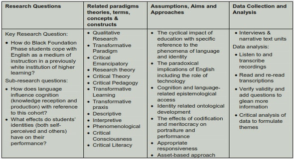
1.INTRODUCTION
1.1 BACKGROUND
1.2 PURPOSE
1.3 RESERACHQUESTIONS
1.4 DELIMITATIONS
1.5 OUTLINE
2.THEORETICAL BACKGROUND
2.1 CAPACITORS.
2.2 ALUMINUM CAPACITORS
2.3 ELECTRO CHEMICAL ETCHING PROCESS.
2.4 ANODIC OXIDE FORMING PROCESS
2.5 EIS (ELECTRO CHEMICAL IMPEDANCE SPECTROSCOPY).
2.6 CPE (CONSTANT PHASE ELEMENT).
3.METHOD AND IMPLEMENTATION
3.1 GROUP 1 – IN HOUSE SAMPLES
3.2 GROUP 2 – INDUSTRIAL SAMPLES (BOTH ETCHED & FORMED ANODIC INDUSTRIALLY)
3.3 GROUP 3 – INDUSTRIAL SAMPLES OF 90 MICRONS THICKNESS
3.3.1 SET-1- FORMING IN 7% wt BORIC ACID
3.3.2 SET-2- FORMING IN ALL 3 DIFFERENT ELECTROLYTES
3.3.3 SET-3- FORMING IN ONLY BORIC ACID & AMMONIUM PHOSPHATE
4. FINDINGS AND ANALYSIS
4.1 DIFFERENT SAMPLES FINDINGS AND ANALYSIS AND THEIR MORPHOLGY
4.1.1 GROUP 1- ANALYSIS OF IN HOUSE ETCHED SAMPLES
4.1.2 MORPHOLOGY OF E8 SERIES SAMPLES
4.1.3 ANALYSIS OF E8 SERIES SAMPLES DATA .
4.1.4 ANALYSIS OF INHOUSE ETCHED AND FORMED SAMPLES DATA .
4.1.5 MORPHOLOGY OF THE IN HOUSE ETCHED AND FORMED SAMPLES
4.1.6 ANALYSIS OF EIS DATA OF IN HOUSE ETCHED AND FORMED SAMPLES
4.2 GROUP 2 – ANALYSIS OF INDUSTRIAL SAMPLES.
4.3 GROUP 3 – ANALYSIS OF INDUSTRIAL SAMPLES OF 90 MICRONS THICKNESS.
4.3.1 ANALYSIS OF EIS DATA OF 90 MICRONS THICK FOIL .
4.3.2 MORPHOLOGY OF 90 MICRONS THICK FOIL FORMED IN 15%WT AMMONIUM ADIPHATE
4.3.3 MORPHOLOGY OF 90 MICRONS THICK FOIL FORMED IN 7% WT BORIC ACID
4.3.4 MORPHOLOGY OF 90 MICRONS THICK FOIL FORMED IN 1.5%WT AMMONIUM PHOSPHATE
4.4 COMPARISON OF MORPHOLOGIES OF 3 DIFFERENT GROUP SAMPLES.
5. DISCUSSIONS AND CONCLUSIONS
6. REFERENCES.
7. SEARCH TERMS
8. APPENDICES.
9. LIST OF FIGURES.
10.LIST OF TABLES
GET THE COMPLETE PROJECT
Electrochemical etching and anodizing as key stages of surface treatment of aluminium foil for electrolytic capacitor industry