Get Complete Project Material File(s) Now! »
Silicon Solar Cells: How to be valuable when approaching the theoretical limit?
As for solar modules, the three main parameters of a solar cell are efficiency, cost and reliability. In terms of reliability, the efforts to increase the lifetime of modules are often focused on the glass, the encapsulant, the by-pass diodes or the frame. Those items aim at protecting the solar cell from external degradation phenomena (e.g. mechanical, UV exposure, humidity). Despite these protections, the solar cell itself can degrade with time. The most common degradation of crystalline silicon cells is due to the UV exposure [25], cracking due to mechanical or thermal stresses [26], corrosion of electrical contacts [27] and hot spot heating [28]. The attention on solar cells reliability is all the more important that the failure of a single cell leads for the whole module to fail because the poor cell will dissipate the extra power of the rest of the cells. Therefore, an homogeneity of solar cells behavior has to be achieved. In order to fully understand degradation phenomena, nano-scale characterization techniques can be valuable. For example, in the case of UV degradation, it has been shown that the nanometric antireflective layer SiNx is affected and the interface with the crystalline silicon is degraded [25]. Nano-scale investigation techniques enable to analyze the interfaces and their homogeneity along the wafer cross-section. Metal/Semiconductor interfaces investigation would also be of interest in the case of the corrosion of contacts for instance. Regarding the efficiency, the first and second generations are single junction solar cells. This means that only one kind of material is used to absorb the light. All the incident photons on a single junction solar cell cannot convey all their energy to the electrons because the low energy photons are not absorbed by the cell and high energy photons energy is transformed only partially into electric energy. In 1961, William Schockley and Hans Queisser demonstrated that the maximum achievable efficiency for a single junction solar cell is 33% [29]. In the case of silicon which bandgap is not optimal and presents inherent losses, the maximum achievable efficiency is estimated at 29%. In 2016, Kaneka announced a laboratory record of 26.33% with a single junction silicon solar cell (IBC heterojunctions) [30]. Thus, the gap between theory and experiments for single junctions is narrowing down to a mere 3.4%. These losses are composed of optical losses and electrical losses: resistive or recombination losses. For both kinds of losses, the improvements in the industry are expected in a near future. These improvements are well summed up in the ITRPV report [31]. For instance, to reduce optical losses, the trend toward putting the two contacts at the back of the cell (back contact solar cells) may increase from less than 5% of the market today to 20% in 2025. These cells sometimes face series resistance issues due to issues of contacting. In these cases of investigation, having a nano-scale resolution can be very useful. In order to reduce the electrical losses, different strategies include new processes for wafers (new crystallization [32] and new sawing techniques), new strategies for doping the wafers (decreasing sheet resistance of contacted parts and new doping techniques), new contacting techniques to achieve low recombination contacts and new passivation techniques to reduce the defects responsible for recombination on the two sides of the wafers. Even when using new processing techniques, some defects are still remaining. For instance, in n-type crystalline silicon wafers, some atomic dislocations have induced parasitic electrical effects [33]. These are all short to midterm strategies. At long term, the necessity to go beyond the Schockley Queisser limit while being cost competitive seems inevitable. To achieve this objective, the most likely way is to go toward a double junction with another material. Many materials, such as perovskites, CZTS or GaAs are under investigation worldwide but for the moment, no solution is mature enough in a midterm perspective. For these multi-junction technologies, nano-scale analysis of interfaces between materials is crucial to check the electrical properties and their homogeneity [34].
Given that efficiency improvements are limited to 3.4% at midterm perspective, cost improvements represent the main overall challenge for crystalline silicon solar cells. Different strategies of cost reduction are considered. The reduction of wafer thickness is one of the most important. According to ITRPV, the average wafer thickness in industry should decrease from 180 μm in 2015 to 120 μm in 2025 [31]. More aggressive strategies using bottom up epitaxial silicon aim at producing wafers 50 μm thick or below [35], [36]. At LPICM, an expertise on low temperature epitaxial silicon solar cells has been built [37], [38]. To increase the absorption of these cells, improvement on light trapping has to be achieved. This can be performed by using nanophotonics concepts, which was the ambition of the European project PhotoNvoltaics [39], [40] and French project Nathisol [41]. Light trapping can be obtained using photonic crystals [42] or nano-texturing. In the case of nano-texturing, the use of nano-scale characterization techniques is obvious. Nanostructuring techniques are sometimes aggressive and create nano-scale defects that have to be investigated. Other cost reduction strategies include the reduction of the costs of contacts. One example is the amount of silver per cell. A decrease from 0.10 g/cell in 2015 to 0.04 g/cell in 2025 is expected. Other materials such as copper are also considered to replace silver. Another example is the use of new metallization technologies and to reduce the contact fingers width [31]. Finally, improvements in the throughput of equipments at all solar cell process steps are expected, making future cells more cost competitive. All the difficulty is to be able to reduce costs while preserving efficiency and reliability. Therefore, any change in the production line may induce new sources of performance or reliability drop. Investigation of these drops is crucial to start a new optimization of processes enabling to achieve a new efficiency-cost-reliability optimum.
While mapping the different perspectives for future crystalline silicon solar cells improvement, we concluded that nano-scale analysis could help understanding degradation phenomena and detect defects in new designs that aim at improving efficiency and reducing cost. The closer from the limit we get, the harder the implementation of novel solutions on crystalline silicon solar cells are. In that perspective, developing new nano-scale characterization techniques designed for specific photovoltaic problematic is important. In the following part, we will discuss the recent evolution of a young family of microscopy techniques called scanning probe microscopy. It enables new nano-scale measurement on solar cells which were not possible with traditional optical and electronic microscopy techniques before.
Scanning Probe Microscopy: “Feeling” the surface at the nano-scale.
“For scanning tunneling microscopy, we brought along some experience in tunneling and angstroms but none in microscopy or surface science. This probably gave us the courage and light-heartedness to start something which should “not have worked in principle” as we were so often told. “ Gerd Binnig and Heinrich Rohrer, Nobel Lecture, December 8th 1986 – Scanning Tunneling Microscopy from Birth to Adolescence. In 1986, Gerd Binnig and Heinrich Rohrer received the Nobel Price for the invention of the scanning tunneling microscope (STM) which dazzled the world in 1981 with the first real-space images of the surface of silicon. Not only this invention enabled to perform surface measurements with a resolution which was unachievable at that time, but it also paved the way for a new family of microscopy techniques called “scanning probe microscopy” (SPM) which enables today to perform a broad range of measurements (e.g. electrical, chemical, thermal) at the nano-scale on the surface of all kinds of materials.
In nano-scale research, three families of microscopies are used: optical microscopy, electron microscopy and scanning probe microscopy. In optical and electron microscopies, a beam of carriers, either photons or electrons are focused on a spot of the surface to be analyzed. Because the wavelength of these carriers is below the micrometer, these techniques enable researchers to see at the nano-scale. The information on the surface is extracted from the reflected or transmitted carriers. This is exactly the mechanism used by the human eye to see an object by interpreting the intensity of detected photons. In the case of scanning probe microscopy, images of surfaces are performed using a physical nano-probe that scans the surface. Therefore, scanning probe microscopy is very similar to feeling or touching the surface at the nano-scale. For the three microscopy techniques, surface roughness can be seen. However, the way to get it is different. This induces pros and cons for each of these techniques. Optical microscopy is the oldest family of microscopies. The development of modern optical microscopy took place in the middle of the 19th century. It is the only microscopy technique that enables real color imaging. It also has the advantage of being versatile, fast and to require no sample pre-treatment. However, its lateral resolution is limited by the diffraction limit to more than a hundred of nanometers. Recently, some progress has been made to go below the 100nm resolution using holography or fluorescence for instance, but these techniques remain so far limited to niche applications. In order to reach resolutions below 100nm, shorter wavelengths than the traditional one used in optical microscopy can also be used. High energy electrons can reach much shorter wavelengths that enable resolution below one Angstrom. For instance, using a 20 kV electron gun, the electron spot can reach down to 0.3 Angstroms. Electron Microscopy was invented in 1931 by two German scientists: Max Knott and Ernst Ruska [43]. Ernst Ruska was awarded the Nobel Prize in 1986, the same year as Gerd Binnig and Heinrich Rohrer. Transmission electron microscopy (TEM) was developed first because the resolution for scanning electron microscopy (SEM) was limited at that time to 100 μm [38]. The first transmission electron microscope was built in 1933 [43] and the first commercial TEM was available in 1939 for which a resolution of 2 nm was claimed [43]. Because it was difficult to compete with the resolution of TEM, it took a long time for the community to understand the interest of scanning electron microscopy. The first true SEM was developed by Zworykin in 1942 and reached a resolution of 50 nm. It took more than 20 years of resolution improvements to convince the scientific community of the interest of SEM. In 1965, the first commercial SEM was presented by Cambridge Scientifc Instruments [44] with a resolution of 10 nm. Since then, the number of publications using SEM has overcome that using TEM, as Figure 1.5 shows. SEM offers the advantage of analyzing all kind of samples: conductors, semiconductors or insulators (covered with stain coating). It does not require a major surface preparation step. However, its resolution is limited to a few nanometers which is one to two order of magnitudes better than optical microscopy but also one to two orders of magnitude worst than TEM and scanning probe microscopies. Indeed, TEM can reach resolutions close to the Angstrom (<0.2 nm) enabling direct imaging of crystalline lattices, which is used to delineate defects inside the sample for instance. However, the preparation of samples for TEM is complicated and time consuming because a long preparation is required to make the samples atomically thin.
STM, AFM & the wide family of AFM extensions
The two main reasons behind the birth of scanning probe microscopy techniques at the beginning of the 1980s were the maturity of tunneling experiments and the availability of piezoelectric devices.
Even though the principle of tunneling effect was discovered in 1903, the acceptance of electron tunneling in solids happened in the late 1950s with the first studies on semiconductors. Vacuum tunneling spectroscopy measurements took time to develop because of experimental hurdles, mainly vibration problems. In 1981, G. Binnig et al. showed the feasibility of vacuum tunneling with modest means. The suppression of vibrations was achieved by soft suspension of a compact tunneling unit [47]. Given this result, mapping of tunneling signal was achieved with the use of a piezoelectric actuator which enables motions of the scanning tip below the nanometer. Despite the fact that piezoelectricity found its first applications at the beginning of the 20th century, the spreading of piezo devices only happened in the 1970s when Japanese companies and universities formed a “competitively cooperative association” which aimed at developing knowledge, new applications, new processes, and new commercial markets for piezoelectric devices in a coherent and profitable way. This lead to the development of new piezoresistive families which were both competitive and free of patents. Those actuators were used in the first scanning probe microscopes.
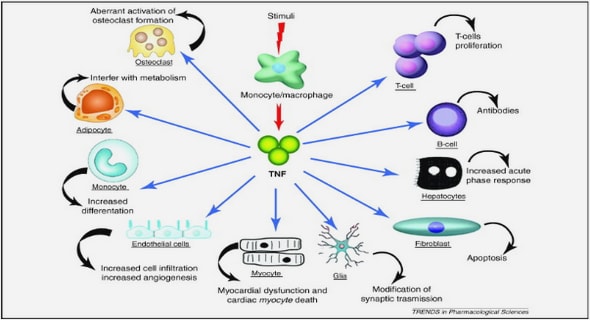
In 1981, G. Binnig and H. Rohrer introduced the Scanning Tunneling Microscope (STM), which was the first instrument to generate real-space imaging of surfaces with atomic resolution. Their key success was to introduce a feedback loop to regulate the distance between the sample and the probe. STM was the first scanning probe microscopy technique and it paved the way for a wide family of scanning probe microscopy techniques, as Figure 1.6 shows. Following the STM, two topographical scanning probe microscopies rose up: the scanning near field optical microscope (SNOM) and the atomic force microscope (AFM). The SNOM uses near field optics below the scanning tip to perform optical images with a resolution lower than the wavelength λ, typically λ/20. The AFM uses the forces between the tip and the sample to make a 3D image of the surface at the nano-scale. The motion is monitored by the reflection of a laser beam on the tip which is recorded by a photodetector. The great advantage of AFM compared to STM is that it is not limited to electrically conductive surfaces to get a tunneling current. AFM is a material agnostic technique. It was invented in 1986 by G. Binnig, C. Gerber and C.F. Quate and became commercially available in 1988. During an AFM scan, several kinds of interactions can be recorded along with the topographical image. For instance, electrostatic or magnetic forces can interact with the probe while scanning. An SPM extension is a manner of using these interactions to map a signal. Shortly after the invention of AFM, a wide range of SPM techniques was developed enabling nano-scale imaging of thermal, piezoelectric, mechanical, chemical, magnetic and electrical properties (see Figure 1.6). The principle of these techniques is the same: the AFM probe makes it possible to transfer an existing macro-scale technique to a nano-scale one. However, quantitative analysis at nano-scale is challenging to achieve because many additional artefacts take place, such as correlation of the measurement to the topography or local tip-induced oxidation. Therefore, interpretations of nano-scale SPM measurements are sometimes challenging and some SPM extensions remain qualitative. Improvements of SPM extensions are still underway with qualitative measurements at nano-scale already giving insightful information in several research fields.
Table of contents :
Chapter 1 – Context
1.1 Crystalline silicon solar cells
1.1.1 Solar: A super-abundant source of green power
1.1.2 Photovoltaics: From a scientific curiosity to a bankable energy solution
1.1.3 Silicon Solar Cells : The unassailed first generation
1.1.4 Solar cells: one of the many pieces of the photovoltaics puzzle
1.1.5 Silicon Solar Cells: How to get more valuable when approaching the theoretical limit?
1.2 Scanning probe microscopy
1.2.1 Scanning Probe Microscopy: “Feeling” the surface at the nano-scale
1.2.2 STM, AFM & the wide family of AFM extensions
1.2.3 Electrical Extensions: Putting on the right glasses for solar cell investigation
Chapter 2 – Experimental Background
2.1 Atomic Force Microscopy
2.2 Kelvin Probe Force Microscopy
2.2.1 Basic Principles
2.2.2 AM vs FM mode
2.3 Conductive Probe AFM
2.4 Electron Microscopy: SEM and EBIC
2.5 Investigated Samples and Solar Cells
2.5.1 Passivated Crystalline Silicon Wafers
2.5.2 Calibration Samples
2.5.3 Epitaxial Silicon Solar Cells
2.5.4 Interdigitated back contact solar cells
Chapter 3 – Weaknesses of KPFM and CP-AFM techniques
3.0 Introduction
3.1 Parasitic Illumination from AFM laser
3.2 Tip-induced surface degradation
3.2.1 Tip-induced oxidation
3.2.2 Nano-Scratching
3.2.3 Tip-induced surface band bending
3.3 Tip degradation during scans
3.3.1 Tip coating degradation
3.3.2 Tip Contamination
3.4 Convolution to topography
3.5 Stray Capacitances
3.6 Thermal Noise
3.7 Limited scan speed, size and height
3.8 Surface dependence
3.9 Conclusion
Chapter 4 – Strengths of KPFM and CP-AFM techniques
4.0 Introduction
4.1 Spatial Resolution
4.2 Sensitivity to illumination
4.3 Low charging effect and activation
4.4 Direct Electrical Measurements
4.5 Versatility
4.6 Acquisition time and dynamic measurements
4.7 Conclusion
Chapter 5 – Material Investigation
5.0 Introduction
5.1 Doping measurements at the nano-scale
5.1.1 Context
5.1.2 Our approach
5.1.3 Results
5.2 Lifetime measurement at the nano-scale
5.2.1 Context
5.2.2 Our approach
5.2.3 Results
5.3 Conclusion
Chapter 6 – Devices Investigation
6.0 Introduction
6.1 Devices investigation under electrical bias
6.1.1 Measurements under constant electrical bias
6.1.2 Electric field investigation
6.1.3 Measurements under modulated frequency electrical bias
6.1.4 Conclusion
6.2 Devices investigation under illumination
6.2.1 Measurements under different illumination intensities
6.2.2 Measurements under different illumination wavelengths
6.2.3 Conclusion
6.3 Conclusion
Chapter 7 – Conclusions and perspectives
7.0 Introduction
7.1 Take-away messages
7.2 Perspectives: Our “ideal” microscope to investigate solar cells
7.2.1 Features of both microscopes
7.2.2 Features specific to OM/SPM
7.2.3 Features specific to EM/SPM
7.3.3 Conclusion
References