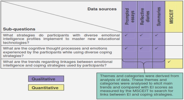
Get Complete Project Material File(s) Now! »
Chapter 3 Defects in Semiconductors
Introduction
In an ideal crystal lattice, each atom is at its designated position and deviations from this perfect structure are called imperfections or defects. These defects may introduce electronic energy states into the semiconductor band gap, which can be placed into two categories: shallow levels and deep levels. Shallow levels are located near their related band edges (valence band for acceptors and conduction band for donors) i.e. ~0.1 eV from the band edge, thus these levels are thermally ionized at room temperature. The ionization energy of a shallow level can be approximately described by a modified hydrogenic model [1]. For example, a shallow donor resembles a hydrogen atom with a positive nucleus binding an electron. Impurity elements which are used as dopants in semiconductors normally create these shallow levels which are ionized at room temperature and provide free carriers to form p-type or n-type semiconductor. Deep levels are those defects positioned deeper in the band gap than the dopant levels and are found to bind the carriers much more strongly into highly compact, localized states. The deep levels have higher ionization energies, therefore contribute very little to the free charge carriers. Defects with deep levels in the band gap are often referred to as, ‘traps’, ‘recombination centers’, or ‘generation centers’. Deep levels are important in semiconductors since they modify the properties of the semiconductors and therefore, those of the devices fabricated thereon. Deep levels are desirable in some applications, e.g. in fast switching devices, where they can be exploited as recombination centers which quickly remove minority carriers, enhancing the device’s switching speed thereby increasing efficiency [2,3]. Deep levels may also be a nuisance if present in semiconductors that are used for photovoltaic applications since they reduce the cells’ efficiency by allowing created electron-hole to recombine. Thus deep level study is of paramount importance in the semiconductor device industry so that those deep levels which are useful can be deliberately added and those that are deleterious can be reduced or eliminated. This chapter will outline the common properties of deep levels (i.e. structure, charge states, formation and migration mechanisms) in silicon and germanium.
Primary Defects
Defects in semiconductors can be divided into two main categories; point defects and extended defects. Point defects are not extended in space in any dimension and this implies that the perturbation of the lattice is localized about a lattice site and involves only a few nearest neighbours. There are two kinds of point defects of great interest in semiconductor crystals, intrinsic (e.g. vacancies or self-interstitial) and extrinsic point defects (e.g. impurity atoms occupying substitutional or interstitial lattice sites. Small agglomerations of several point defects like divacancies, vacancy-impurity complexes, vacancy-donor etc are also generally considered as point defects. Extended defects are extended in nature (such as, grain boundaries, dislocations or stacking faults). The discussion in this section is focussed more on point defects which are more relevant to the work covered in this thesis.
Vacancy Defect
If an atom is removed from its regular lattice site the empty lattice site is called a vacancy defect (V), and is shown in Fig. 3-1. The vacancy in some semiconductors (e.g. in Ge and Si) can have up to five charge states, V++, V+, V0, V– and V=. In order to form a vacancy by removing an atom from its lattice site four bonds are broken in a diamond crystal structure as shown in Fig. 3-2a [4,5]. The broken bonds can form new bonds depending on the charge state (i.e. which is just the number of electrons occupying the dangling bonds) of the vacancy (Fig. 3-2b and c). This causes small inward and outward displacement of neighboring atoms, which either preserves the local symmetry (relaxation) or alters it (distortion). The amplitude of the displacements depends on the charge state of the defect. Another geometric configuration for describing a vacancy is the ‘split-vacancy’. The ‘split-vacancy’ results when an atom resides at the bond center between the empty sites [6], Fig. 3-2d. The ‘split-vacancy’ is often important primarily to help describe the transition state in vacancy migration [7]. The lattice relaxation depends on the charge state of the point defect (Jahn-Teller effect). Jahn-Teller effect is simply a geometrical distortion which occurs when the electronic state is degenerate, in which case the nuclear state is unstable. Atomic displacements always exist which by lowering the symmetry, split the degenerate level.
It should be noted there is general agreement in defect modeling studies that the vacancy formation energy in germanium (1.7 eV – 2.5 eV) is significantly smaller than in silicon (~4.0 eV), for all charge states. When two neighboring atoms are removed and also when two migrating vacancies meet and combine a divacancy is formed. A divacancy can also exist in four different charge states in Si [8Interstitial Defect
Interstitials are atoms, which occupy a site in the crystal structure, which is not a regular lattice site as shown in Fig. 3-1. An interstitial defect can be of the same species as the atoms of the lattice (self-interstitial) or of a different nature (an interstitial impurity). Interstitials are generally high-energy configurations. Once again, the introduction of an interstitial induces a relaxation and distortion of the lattice, which surrounds it. The type of configuration the interstitial assumes depends on its ability to make bonds with its neighbors and therefore can change with its charge state. A nearby interstitial defect and vacancy defect is called a Frenkel pair.
Secondary Defects
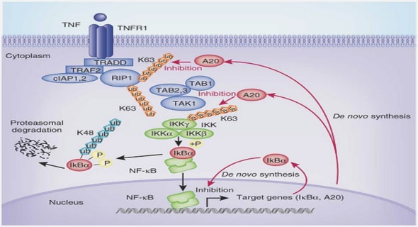
The isolated lattice vacancy (V) and self-interstitial (I) are primary defects produced after high-energy particle irradiation in semiconductors. The primary defects are mobile at low temperatures, e.g. in Si the vacancy becomes mobile above 150 K – 200 K and the interstitial is mobile even at 4.2 K [8]. Therefore, deep level transient spectroscopy measurements of room temperature irradiated silicon will not reveal an isolated vacancy or silicon interstitials. The V and I which survive the recombination of simple defects can diffuse into the semiconductor and interact with other intrinsic and extrinsic defects giving rise to complex room temperature stable defects, some of which are depicted in the schematic diagram shown in Fig. 3-3. For example, in silicon when a vacancy becomes mobile, it can be trapped by an oxygen atom to form a V-O complex (A-center), or the doping impurity (e.g. P) to form a V-P complex (E– center), or by another vacancy to form divacancies. Other complex defects are via the mobile interstitial (I). It is expected that room temperature defect evolution in silicon shown in Fig. 3-3 should hold similarly for germanium.
The Divacancy
The divacancy is formed by the removal of two neighbouring atoms. Generally divacancies can be created in semiconductors by particle irradiation either as a primary defect, when collision cascade is dense enough, or as a secondary defect by pairing of single vacancies diffusing randomly. The vacancy in germanium is negatively charged in a broad interval of Fermi level position in the band gap, therefore the formation of divacancies by pairing of single vacancies is suppressed by the coulombic repulsion of the vacancies [9]. The divacancy in Ge has not yet been identified by experimental techniques. Using density functional theory (DFT) cluster calculations, Janke et al [10] estimated the energy barrier for migration and dissociation of the divacancy. The dissociation energy consisting of the binding energy between two vacancies and the migration of a single vacancy was found to be between (1.5-1.7) eV whereas the migration barrier of the divacancy was found to be 1.1 eV. This corresponds approximately to a thermal stability of 420 K. The divacancy in silicon is well known, and can appear in four charge states, V+ , V0 , V-
The E–center
The E-center can be described as a vacancy trapped next to a substitutional donor atom. The E-center can be formed as a primary defect or when the impurity atom captures a mobile vacancy. As to the formation of an E-center, although local atomic strain effect may need to be considered, the key role is played by the coulombic interaction between a positively charged antimony and a negatively charged vacancy [11]. Let’s consider the E-center in phosphorus-doped silicon, V-P. In the neutral charge state i.e. PV0, two of the three silicon atoms surrounding the vacancy pull together to form an electron pair, leaving an unpaired electron in the orbital of the third silicon atom, while two electrons with antiparallel spins are accommodated by the phosphorus atom. When the Fermi level is above the E-center an extra electron is accepted and becomes negatively charged, PV¯. The formation of E-center in silicon removes two electrons in the conduction band by converting a positively charged P donor atom to a negatively charged V-P center. The formation of the E-center is regarded as an intermediate step in dopant diffusion in silicon and germanium [12].
3.3.3 The A-center
The A-center (V-O) may be regarded as a vacancy trapped next to an oxygen atom in an interstitial position. Similar to the E-center the A-center can be formed as a primary defect or when an oxygen impurity traps a mobile vacancy. The A-center competes for the vacancies with the E-center and its concentration is dependent on the relative O impurity concentration in the sample. The A-center has also been found to be an efficient recombination center [13], and therefore can be used as to control minority carrier lifetime in silicon for fast switching device application.
Other Complex Defects
The mobile Si interstitial (I) diffuses and will replace either carbon (C) or group III impurities e.g. boron (B) (depending on the relative concentration of the two species) through the Watkins replacement [14,15] to form interstitial carbon (CI) or interstitial BI respectively. The CI or BI are mobile at room temperature and will eventually form defect complexes with other impurities {e.g. interstitial boron – substitutional boron (BI-Bs), interstitial boron – interstitial oxygen (BI-OI), interstitial boron – substitutional carbon (BI-Cs), interstitial carbon – interstitial oxygen (CI-OI) or interstitial carbon – substitutional carbon (CI-Cs)} as shown in Fig. 3-3. For a particular defect with a large concentration, it tends to aggregate as the temperature increases from room temperature. In case of a divacancy, when mobile or after dissociating, it can form trivacancies, quadrivacancies, pentavacancies, and higher order defects. This behavior should also be true for self-interstitials and for any type of extrinsic defects.
Most of the primary and secondary defects discussed in the previous sections are electrically active and introduce deep levels in the semiconductor band gap. A deep level may act as a minority carrier trap, majority carrier trap or recombination centre depending on its position in the band gap and on relative capture cross-section of minority and majority carriers. A majority carrier trap is an electron trap in n-type semiconductor or a hole trap in p-type semiconductor. Conversely a minority carrier is a hole trap in n-type semiconductor or an electron in p-type semiconductor. If a majority- or minority- carrier lives a mean lifetime in the captured state and is thermally ejected to the band from which it came, the center may be regarded as majority carrier trap or minority carrier trap respectively. From defect spectroscopy measurements such as deep level transient spectroscopy (DLTS) it is possible to extract the defect properties such as the concentration, energy level, and capture cross-section of defect level. The capture cross-sections, σmajority and σminority can now be used to deduce whether the defect will act as minority carrier trap, majority carrier trap or a recombination centre.
Recombination centers are deep levels with approximately equal capture cross- sections for both electrons and holes and these centers are normally located near the middle of the band gap. After capturing a majority carrier, if the majority carrier stays trapped at the center long enough for the trap to capture a minority carrier, then recombination takes place and the center is acting as a recombination center. Most of the defect spectroscopy techniques measure the defect concentration, energy level, and capture cross section for majority and minority carrier traps, e.g. when using DLTS, all the detected defects are in a situation where they behave as majority or minority carrier traps. Hence it is difficult to say which of the detected defects will be a recombination center. There have been attempts to improve on the technique used to distinguish traps from recombination centers. Markvart et al [16] developed an improved version of DLTS, known as recombination DLTS that can be used to identify defects that act as recombination centers. These centers act as “stepping stones” for carriers and contribute to the current-voltage characteristics of rectifying junctions at a recombination rate, U given by [3,17]
Chapter 1: Introduction
Introduction
References
Chapter 2: Semiconductor Theory
2.1 Introduction
2.2 The Crystal and Band Structure of Si and Ge
2.3 Metal – Semiconductor Junctions
2.3.1 Schottky Barrier Junctions
2.3.2 Depletion Layer
2.3.3 Ohmic Contacts
2.4 Current Transport Mechanism in Metal – Semiconductor Junctions Reference
Chapter 3: Defects in Semiconductors
3.1 Introduction
3.2 Primary Defects
3.2.1 Vacancy Defect
3.2.2 Interstitial Defect
3.3 Secondary Defects
3.3.1 The Divacancy
3.3.2 The E-Center
3.3.3 The A-Center
3.3.4 Other complex defects
3.4 Theory of Displacement of Atoms in Solids
3.4.1 Energy-Loss Mechanisms
3.4.2 Defect Production by Irradiation.
3.4.3 Defect Annealing Mechanisms
References
Chapter 4: DLTS and Laplace-DLTS Aspects
4.1 Introduction
4.2 Emission and Capture of Carriers from Deep Levels
4.3 Deep Level Transient Spectroscopy (DLTS)
4.3.1 Capacitance Transient Processing
4.3.2 DLTS Principles
4.3.3 Defect Depth Profiling
4.4 Laplace-DLTS
4.4.1 Laplace-DLTS Principles
4.5 Electric Field Effect
References
Chapter 5: Experimental Techniques
5.1 Introduction
5.2 Sample Preparations
5.2.1 Silicon Cleaning Process
5.2.2 Germanium Cleaning Process
5.2.3 Ohmic and Schottky Contact Fabrication
5.3 Sample Irradiation
5.3.1 Electron Irradiation
5.3.2 Low Energy Noble Gas Irradiation
5.4 Electrical Characterization Techniques
5.4.1 Current-Voltage & Capacitance-Voltage Measurement System.
5.4.2 Deep Level Transient Spectroscopy and Laplace-DLTS Systems
5.5 Annealing Apparatus
References
Chapter 6: Results
Radiation-induced defects in Ga- or B-doped silicon by 1 MeV electron irradiation
6.1 Introduction
6.2 Experimental Procedure
6.3 Results
6.4 Summary and Conclusion
References
List of Publications
Chapter 7: Results
Defects introduced in n- and p-type Si during contacts fabrication by electron beam deposition (EBD)
7.1 Introduction
7.2 Experimental Procedure
7.3 Results
7.4 Summary and Conclusion
References
List of Publications
Chapter 8: Results
Radiation-induced defects in antimony-doped Ge after electron irradiation
8.1 Introduction
8.2 Experimental Procedure
8.3 Results
8.4 Summary and Conclusion
References
List of Publications
Chapter 9: Results
Defects introduced in antimony-doped germanium during metallization by electron beam deposition
9.1 Introduction
9.2 Experimental Procedure
9.3 Published and other Results
9.4 Summary and Conclusion
References
List of Publications
Chapter 10: Results
Defects introduced in antimony-doped germanium after sputtering by 3 keV Arions
10.1 Introduction
10.2 Experimental Procedure
10.3 Results
10.4 Summary and Conclusion
References
List of Publications
Chapter 11: Conclusions
GET THE COMPLETE PROJECT