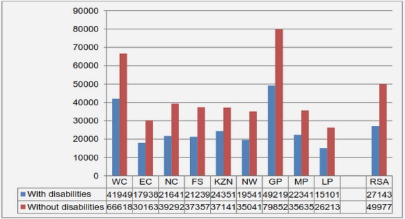
Get Complete Project Material File(s) Now! »
DLTS: Deep level transient spectroscopy
Deep levels in semiconductors influence both the electrical and the optical properties of the material.There are a number of optical techniques for the characterisation of deep level defects in semiconductors. However, one of the main shortcomings of these techniques is that they cannot measure or predict the electrical properties. Since most semiconductor applications rely on the electrical properties of the semiconductor, it is important to know the electrical properties of a deep level defect. Furthermore, many of the processes that occur in deep levels that influence device performance are nonradiative, and cannot be observed by optical techniques. Deep level transient spectroscopy (DLTS) is one of the most versatile techniques used to determine the electrical properties of defects.
The DLTS technique
As described by Lang (1974), the DLTS technique uses a fast, sensitive capacitance meter to measure the capacitance of a reverse-biased Schottky, MOS or p-n junction. According to Equation (2.11), the capacitance of a reverse-biased diode can be related to the width of the depletion region, which in turn depends on the charge in the depletion region, due to dopants as well as deep levels. The DLTS technique measures the change in the capacitance of the junction due to the emission of carriers by defects in the depletion region, as described by Equation (2.29). By processing the capacitance signal with a weighting function, the emission rate of the defect in the depletion region is obtained.Consider the case of a Schottky contact on an n-type semiconductor, as shown in Figure 3.1(A). The semiconductor contains a low concentration of a defect that causes a deep electron trap with energy ET. In the figure the bulk of the semiconductor containing free carriers is indicated by the shaded area,while the depletion region is left unshaded. Filled and open circles indicate filled and empty trapsrespectively. For simplicity, we assume that, initially, all the traps in the depletion region are empty,while all the traps in the bulk of the semiconductor are filled.At the start of the DLTS cycle, a smaller reverse bias (or even a forward bias) pulse is applied across the diode. [Figure 3.1(B)]. This bias pulse reduces the width of the depletion region, increasing the capacitance of the Schottky diode drastically. The reduction in the width of the depletion region fills the traps up to a distance of approximately the depletion width below the surface of the semiconductor.After the filling pulse, the reverse bias is returned to its quiescent level [Figure 3.1(C)]. This increase in reverse bias increases the width of the depletion region again. However, since some of the deep level traps in the depletion region are now filled, the charge density in the depletion region is less than it was in (A), therefore the depletion region is slightly wider and the capacitance slightly lower than was the case in (A).Since the filled traps in the depletion region are above the Fermi level, they now emit carriers by means of thermal processes, as described in Section 2.2. This causes the charge density in the depletion region to increase, reducing its width and increasing the capacitance of the junction. If it is assumed that N N T D ≪ , the depletion region width will not change significantly during the emission of carriers. Under these circumstances, it is reasonable to assume that the emission of carriers from the depletion region may be described by an exponential decay, as in Equation (2.29). The capacitance of the Schottky diode is then also described by an exponential decay function where λ is the decay rate and C∞ is the steady state capacitance of the diode.
If it is assumed that all the defects from the depletion region edge to the interface are filled by the filling pulse and subsequently emptied, the defect concentration may be calculated from the amplitude of the exponential decay function by applying Equation (2.11) It is possible to obtain an activation energy and a capture cross-section associated with the emission of the carriers from the defect by measuring the decay time constant as a function of temperature, as described in Section 2.2.1. In the above explanation, it has been assumed that the defect level is empty in the depletion region and full in the bulk. Since the defect level typically lies much deeper in the band than the dopant level, the defect level intersects the Fermi level a distance λ shallower than the depletion region edge, as shown in Figure 3.2.
Analysis of the DLTS transient
In the idealised case, the DLTS capacitance transient obtained from a sample with a single defect level is an exponential decay function of the form where A is the amplitude, λ is the decay rate and C∞is the capacitance of the junction at equilibrium.
Many physical processes are described by such an exponential decay process, and in principle determining the values of A, λ and C0 is reasonably straightforward.However, it frequently occurs that there is more than one defect level in the semiconductor and that these defects have closely spaced decay constants, or even a continuous band of decay constants. In this case, the capacitance transient can be described as the sum of a number of exponential decay functions.Many techniques have been developed for the deconvolution of such a multi-exponential function.However, there are significant problems associated with all of the techniques, and the analysis generally becomes unreliable in the presence of noise.
1 Introduction
2 Some concepts in semiconductor physics
2.1 Metal-semiconductor junctions
2.1.1 The Schottky model
2.1.2 The ideal case
2.1.3 Behaviour of the barrier under forward and reverse bias
2.1.4 Calculation of the electric field in a Schottky barrier
2.2 Defects and deep levels in semiconductors
2.2.2 Defect occupation as a function of time
2.2.3 Field dependence of the emission rate
3 DLTS: Deep level transient spectroscopy
3.1 The DLTS technique
3.2 Analysis of the DLTS transient
3.2.1 Analogue techniques
3.2.2 Digital processing of DLTS transients
3.3 Differential DLTS
4 Planning of the digital DLTS set-up
4.1 Acquisition of the capacitance signal
4.1.1 Random noise
4.1.2 Response time, sampling rate and resolution
4.1.3 Periodic noise
4.1.4 Stability
4.2 Selection and characterisation of the instrumentation
4.2.1 Digitiser
4.2.2 Capacitance meter
4.2.3 Pulse generator
4.2.4 Rise and fall times
4.2.5 Sample mounting and temperature control
4.3 Other hardware
4.3.1 Fast pulse interface
4.3.2 Synchronisation
4.4 Software
5 Experimental
5.1 Introduction
5.2 Sample preparation:
5.2.1 Gallium Arsenide
5.2.2 Silicon
5.2.3 Gallium Nitride
5.3 IV and CV characterisation
6 Characterisation of the EL2 and E2 defects in n-GaAs
6.1 Introduction
6.2 The EL2 and E2 defect levels in n-GaAs
6.3 Experimental
6.4 Results and discussion
6.5 Conclusions
6.6 Publications
7 Field dependence of the thermally activated emission rate
7.1 Introduction
7.2 Publications
8 DLTS observation of the transformation of bistable defects
8.1 Introduction
8.1.1 Configurationally bistable defects
8.1.2 Charge state controlled metastability
8.1.3 Characterisation of metastable defects
8.1.4 Example: The C–C pair in Si
8.2 Experimental
8.2.1 Introduction
8.2.2 Sample preparation
8.2.3 Determining the defects’ DLTS signatures
8.2.4 Determination of the transformation kinetics
8.2.5 Discussion
8.3 Publications:
9 Negative-U defects in n-GaN
9.1 Introduction
9.1.1 What is U?
9.1.2 Mechanisms leading to negative-U behaviour
9.1.3 Properties of negative-U defects
9.2 DLTS of a negative-U defect
9.2.1 Behaviour of a negative-U defect under changing Fermi level
9.2.2 DLTS of a negative-U defect
9.3 Negative U properties observed in a sputter-deposition induced defect in n-GaN
9.3.1 Introduction
9.3.2 Experimental.
9.3.3 Results and discussion
9.3.4 Conclusion
9.4 Publications
10 Conclusions
References